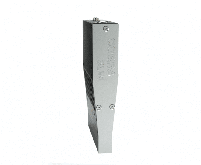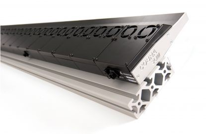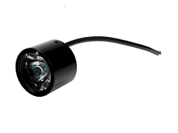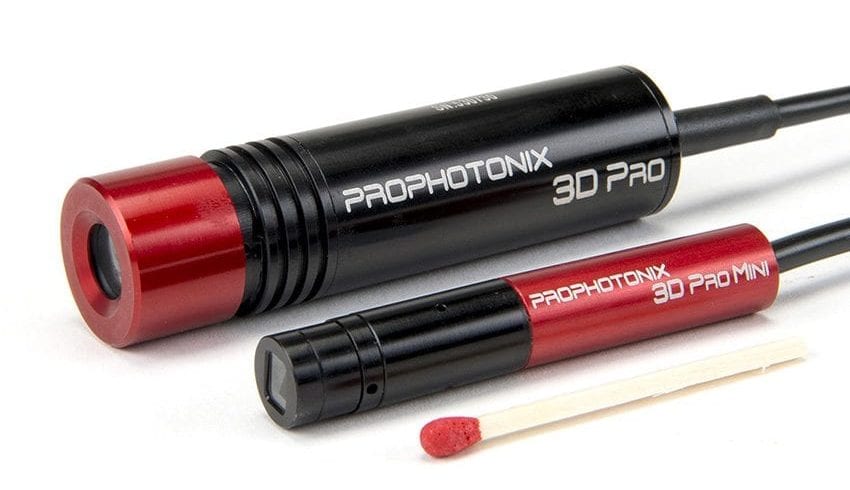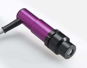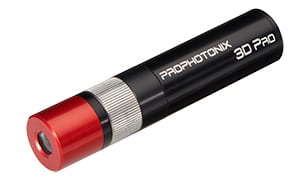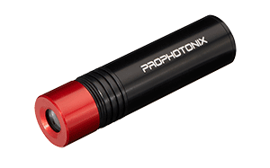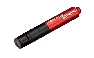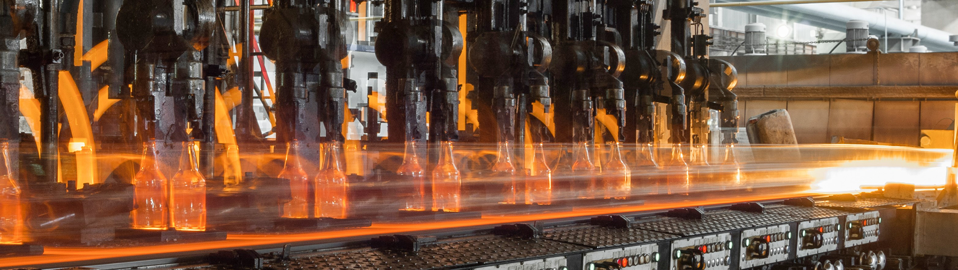
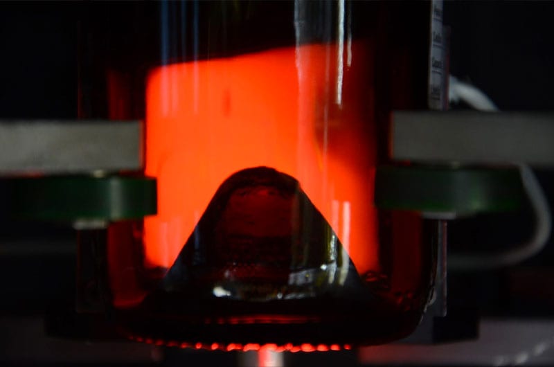
High quality, consistent, and uniform machine vision lighting is essential to a successful vision system. The correct solution raises your throughput rates and improves the level of image detail obtained. ProPhotonix has more than two decades of experience in designing and developing both LED Lights and Structured Light Lasers for machine vision applications.
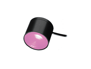
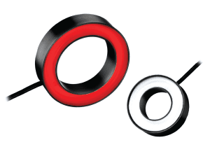
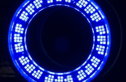
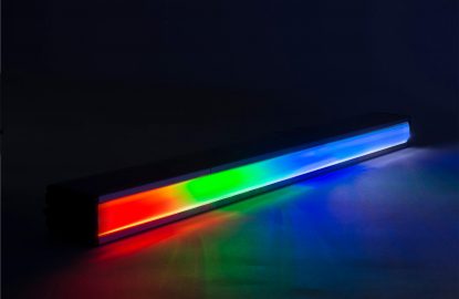
We offer solutions for 3D Imaging, Multispectral Imaging, ANPR (Automatic Number Plate Recognition), IR Machine Vision Lighting, Sorting, and UV Machine Vision Lighting, and many other applications. Our experienced, in-house team of optical, mechanical and electronic engineers can also assist you in developing a custom machine vision lighting solution that will suit your unique application requirements.