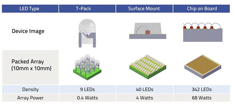
Packaged LEDs
Examples of packaged LEDs are shown in Figures 1 and 2. A packaged LED has an optical lens, bonding wire, electrodes, and resin to encapsulate the LED for protection.
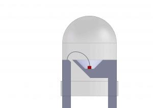
Figure 1: Through hole (T-pack) LED
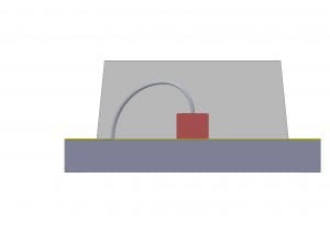
Figure 2: Surface Mount LED
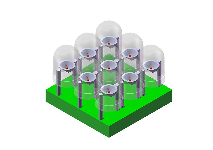
These packages can be affixed to a heat-sinking substrate using either “through hole” mounting or surface mounting. The through-hole mounted devices are often referred to as T-pack LEDs. Arrays built of through-hole LEDs are shown in Figure 3.
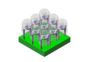
Figure 3: LED Array comprised of T-packs